ASML
PAS 5500
The ASML PAS 5500 is a step-and-repeat projection stepper for photolithography. The PAS 5500 uses reduction optics, typically 5X or 4X, to transfer mask patterns onto wafers. The PAS 5500 family includes i-line (365 nm) and DUV (248 nm) models, with resolutions from 450 nm down to below 200 nm.[1][2][3][4]
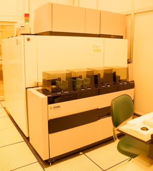
Plate 01PAS 5500 – The Inside Story (1993) | ASML
ASMLWatch on YouTubePlate 02ASML PAS 5500 750 + TEL Act 8 Bundle Available, Wafer size 200mm, Location Asia
delmarphotonicsWatch on YouTubePlate 03ASML's The PAS5500 Revolution | Follow for full video.
Rishi PanchalWatch on YouTube
Wafer size
200mm
Produced
2000–2010
Node / era
280 nm
Performance
Topside and backside alignment[3]
Optics
365 nm[1]
What it is
The ASML PAS 5500 series includes both i-line and deep-ultraviolet (DUV) variants. The PAS 5500/275D is an i-line stepper operating at 365 nm with 280 nm resolution and 40 nm overlay accuracy. The PAS 5500/60 is also an i-line system achieving 450 nm resolution and 90 nm overlay. The PAS 5500/350C is a DUV stepper using a KrF excimer laser at 248 nm, with resolution below 180 nm and overlay below 30 nm. The PAS 5500/300 uses 248 nm DUV light, capable of resolving dense features below 200 nm and isolated lines below 150 nm.[1][2][3][4]
How it works
The PAS 5500 series uses a wafer handler to load wafers from cassettes and a prealigner for centering. The wafer stage, constructed from Zerodur for low thermal expansion, is positioned using multiple interferometers for nanometer-scale accuracy. A level sensor measures wafer height and tilt to maintain focus during exposure. The system can expose fields of various sizes depending on the reticle and lens configuration.[3]
What can it run?
Process applications and technology nodes documented for this tool.
- Measurement calibration patterns
- Gratings and waveguides
- Microelectromechanical systems
- Thermal sensors
Why won't it start?
Documented failure modes, common issues, and field considerations.
- Backside contamination can locally deform the wafer surface and degrade focus/printing quality.
- Wafer stage contamination can result in machine downtime of several days.
- Reticle contamination can cause printing defects and irreversible degradation of printing performance.
What do the numbers mean?
Wafer handling29
- Wafer sizes supported
- 75 mm, 100 mm, 150 mm, 200 mm (PAS 5500/275D); 100 mm default, 150 mm capable (PAS 5500/60); 100 mm default, 150 mm on request, also 4", 6", 8" (PAS 5500/350C)[1]
Optics & imaging54
- Exposure wavelength
- 365 nm (i-line) for PAS 5500/275D and PAS 5500/60; 248 nm (KrF DUV) for PAS 5500/350C[1]
- Reticle size
- 152.40 mm x 152.40 mm (PAS 5500/275D), 5 inch (PAS 5500/60), 6 inch square (PAS 5500/350C)[1]
- Numerical aperture (PAS 5500/350C)
- 0.40 to 0.63 (conventional); up to 0.70 (tunable range)[3]
Performance3
Configuration & options26
- Maximum field size
- 22 mm x 22 mm or 27.4 mm x 14.7 mm (PAS 5500/275D), 18 mm x 22.4 mm (PAS 5500/60), 2.2 cm x 2.2 cm (PAS 5500/350C)[1]
Vintage & configurations
Documented models & variants
| Designation | Generation | Vintage | Changes | Source |
|---|---|---|---|---|
| PAS 5500/275D | i-line | — | High-throughput i-line stepper using 365 nm light; 5X reduction and projection capability; automated wafer handling for substrates from 200 mm diameter wafers down to small pieces. | nist.gov[1] |
| PAS 5500/60 | i-line | — | Automatic 100 mm wafer cassette processing capability; 365 nm near-UV light; minimum feature size of 450 nm; 150 mm capable with advanced notice. | snfguide.stanford.edu[2] |
| PAS 5500/350C | — | 2000–2010 | DUV photolithography stepper using 248 nm KrF laser source; 4x or 5x reduction; high throughput; handles 100 mm wafers by default and 150 mm on request. | epfl.ch[3] |
| PAS 5500/300 | DUV | — | Described as a DUV stepper configured for 4-inch wafers. | wiki.nanotech.ucsb.edu[4] |
| PAS 5500/200 | i-line | — | Described as a 5X reduction, i-line stepper for 6 inch wafers using 6 inch reticles, with 350 nm resolution, 0.48-0.60 variable numerical aperture, 22x22 mm maximum field size, and better than 50 nm overlay capability. | manualslib.com[6] |
| PAS 5500/400 | Step & Scan | 1995 | Described as the second step & scan system released by ASML, with a 4X reduction ratio and maximum long-term mask overlay of 35 nm. | chiphistory.org[5] |
What replaced it?
Alternatives
Tools documented as functional equivalents — same process step and wafer size, from a different manufacturer. Each equivalence cites its source.
- Nikon NSR 2205 i 14 E 2 i-Line— Same function class: Lithography, 200mmCompare in depthsource[1]
- GCA AS200— Same function class: Lithography, 200mmCompare in depthsource[1]
Related models
- predecessorASML PAS 2000— ASML developed the PAS 5500 after the PAS 2000; the PAS 5500 became the company's first commercial breakout.source[7]
Where are the manuals?
Publicly hosted documents referencing this tool, linked at their original location. Hosted by the linked institutions — availability may change.
- DUV Resist InformationDocumentcornell.edu
- SPR 220-3.0Datasheetucsb.edu
- SPR220 (SPR220-3, SPR220-7)Datasheetucsb.edu
Generated from public-source data on file. Enter your email to access — nothing is published; details are routed privately.
Not publicly documented
Field notes
No research found yet — worked with this tool? Share what you know.
Frequently asked questions
What exposure wavelength does the PAS 5500/275D use?
It uses 365 nm wavelength light.[1]
What resolution is given for the PAS 5500/275D?
It is capable of 280 nm resolution.[1]
What substrate sizes are supported on the PAS 5500/275D?
The tool supports 75 mm, 100 mm, 150 mm, and 200 mm wafers, and small pieces can be processed on carrier wafers.[1]
What light source does the PAS 5500/350C use?
It uses DUV light from a KrF laser source at 248 nm.[3]
Not publicly documented
The following facts about the PAS 5500 are absent from this record as of this revision. First-hand knowledge or a citation closes a gap; every submission is reviewed before publication.
The control-system platform and OS era of the PAS 5500 are not on record.
Answerable by: an engineer who operated it or OEM installation records
No publicly documented compatible parts, consumables, or accessories for the PAS 5500 are on record.
Answerable by: an OEM parts catalog or a service engineer
Sources & citations
Sources (11)Every fact above is drawn from these public sources
- [1]nist.gov — nist.govnist.gov
- [2]snfguide.stanford.edu — snfguide.stanford.edusnfguide.stanford.edu
- [3]epfl.ch — epfl.chepfl.ch
- [4]wiki.nanotech.ucsb.edu — wiki.nanotech.ucsb.eduwiki.nanotech.ucsb.edu
- [5]chiphistory.org — chiphistory.orgchiphistory.org
- [6]manualslib.com — manualslib.commanualslib.com
- [7]en.wikipedia.orgen.wikipedia.org
- [8]Equipment Resources | CNF — cnf.cornell.educnf.cornell.edu
- [9]Lithography — tudelft.nltudelft.nl
- [10]ASML PAS 5500/200 – Stepper | UCLA Nanolab — nanolab.ucla.edunanolab.ucla.edu
- [11]ASML: Products - TWINSCAN NXT:1970Ci — asml.com (Sep 15, 2016)web.archive.org
Last updated Oct 8, 2026.
Compare with similar tools
View all →The GCA AutoStep 200 DSW (also known as AS200) is a 5X reduction i-line wafer stepper designed for up to 200mm wafers.

Nikon NSR 2205 i 14 E 2 is an i-line stepper.
The SUSS MicroTec BA8 Gen4 Pro is a semi-automated mask alignment and wafer bonding system for 200 mm wafers, with capabilities including exposure, UV bonding, fusion bonding, imprinting, and selective plasma activation.