Filmetrics
F50
The Filmetrics F50 is an optical film thickness and wafer-mapping tool. The Filmetrics F50 measures thin-film thickness and optical properties using white-light reflection. The Filmetrics F50 supports motorized mapping on wafers up to 150mm.[1][2]
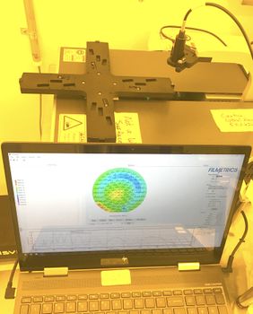
Plate 01Nanometrix - Filmetrics F50
NanometrixWatch on YouTubePlate 02F50 Hardware Installation
FilmetricsWatch on YouTubePlate 03F50 Hardware Installation
TechnolutionsWatch on YouTube
What it is
How it works
The F50 uses white light reflection to measure thin films on substrates.[2]
The F50 measures normal-incidence reflection from the sample surface and uses deuterium and halogen light sources.[2]
The F50 can make single-spot measurements or motorized wafer maps, and the motorized stage acquires reflection spectra at programmed points across the wafer.[2]
The F50 fits the measured reflection data to an optical model to estimate thickness, refractive index, and absorption.[2]
Where it fits in the process flow
The F50 is suited to unpatterned samples, and it can also measure small substrates.[2]
Applications
The F50 measures thickness and optical properties of films on substrates.[2]
The F50 supports mapping of thin films across full wafers.[2]
The F50 can measure reflection spectra from 190 to 1100 nm and can be used for thickness, refractive index, and absorption measurements.[2]
The F50 is best suited to unpatterned samples.[2]
- Thickness and optical property measurements of films on substrates
- Mapping of thin films on full wafers
- White-light reflection-based thin-film reflectometry
What do the numbers mean?
Wafer handling6
Optics & imaging5
Performance1
Control & software2
Configuration & options15
Vintage & configurations
Documented models & variants
| Designation | Generation | Vintage | Changes | Source |
|---|---|---|---|---|
| F50-UV | — | — | Distinguished by wavelength range; described as requiring shorter wavelengths for thinner films. | web.archive.org[3] |
| F50-NIR | — | — | Distinguished by wavelength range; longer wavelengths allow measurement of thicker, rougher, and more opaque films. | web.archive.org[3] |
| F50-EXR | — | — | Distinguished by wavelength range. | web.archive.org[3] |
| F50-UVX | — | — | Distinguished by wavelength range. | web.archive.org[3] |
| F50-XT | — | — | Distinguished by wavelength range. | web.archive.org[3] |
| F50 | — | — | Standard F50 model listed in the archived Filmetrics product page with wavelength range 380-1050nm and thickness range 15nm–70um. | web.archive.org[3] |
What replaced it?
Related models
- siblingFilmetrics F10-RT-UVX— Listed as another Filmetrics optical film thickness tool in the UCSB tool list.source[1]
- successorFilmetrics F60— The source says the F60-t family maps film thickness and index just like the F50 products.source[4]
- siblingFilmetrics F60-t— The F60-t family maps film thickness and index just like the F50 products.source[4]
Where are the manuals?
Generated from public-source data on file. Enter your email to access — nothing is published; details are routed privately.
Not publicly documented
Field notes
No research found yet — worked with this tool? Share what you know.
Frequently asked questions
What does the F50 measure?
The F50 measures film thickness and optical properties on substrates.[2]
What measurement method does the F50 use?
The F50 uses white light reflection at normal incidence.[2]
Can the F50 map wafers?
The F50 can do motorized wafer mapping of optical properties.[2]
What wafer size can the F50 map?
The F50 can perform motorized mapping on wafers up to 150 mm.[2]
What sample types are suitable for the F50?
The F50 is best for unpatterned samples and can also measure small substrates greater than or equal to 2 to 3 mm.[2]
Not publicly documented
The following facts about the F50 are absent from this record as of this revision. First-hand knowledge or a citation closes a gap; every submission is reviewed before publication.
No publicly documented production dates or lifecycle milestones (introduction, end of production, EOL) for the F50 are on record.
Answerable by: OEM historical records or a trade-press announcement
The control-system platform and OS era of the F50 are not on record.
Answerable by: an engineer who operated it or OEM installation records
No publicly documented failure modes or field errata for the F50 are on record.
Answerable by: a field service engineer, process engineer, or maintenance technician
The process node or technology generation of the F50 is not on record.
Answerable by: an OEM datasheet or a fab qualification report
No publicly documented compatible parts, consumables, or accessories for the F50 are on record.
Answerable by: an OEM parts catalog or a service engineer
No research found yet — worked with this tool? Share what you know.
Sources & citations
Sources (5)Every fact above is drawn from these public sources
- [1]Tool List - UCSB Nanofab Wiki — wiki.nanotech.ucsb.eduwiki.nanotech.ucsb.edu
- [2]wiki.nanotech.ucsb.edu — wiki.nanotech.ucsb.eduwiki.nanotech.ucsb.edu
- [3]web.archive.org — web.archive.orgweb.archive.org
- [4]web.archive.orgweb.archive.org
- [5]Tool List - UCSB Nanofab Wiki — wiki.nanotech.ucsb.eduwiki.nanotech.ucsb.edu
Last updated Oct 5, 2026.
Compare with similar tools
View all →
The KLA Alpha Step 500 is a profilometer.
KLA P/N: 0023889-00 is a wafer vacuum chuck compatible with KLA SP1 Classic, SP1-TBi, and SP1-DLS systems.

The KLA SFS 6420 is a wafer inspection system for non-patterned particle detection, compatible with 150 mm and 200 mm wafers, using an Algon laser source.
The KLA .204 PSL Wafer is an 8-inch NIST-traceable reference wafer compatible with Surfscan 6xy0 and Sp1 particle counters.