Olympus
S2-ET
What it is
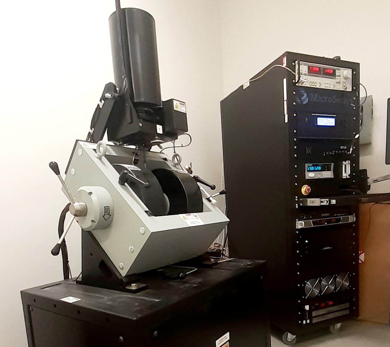
General reference — not yet source-verifiedThe Olympus S2-ET is an optical microscope used for metrology and inspection applications in semiconductor fabrication and materials analysis. Optical microscopes of this class provide magnified bright-field, dark-field, and differential interference contrast imaging for examining surface features, defects, and structures on wafers and other samples.
How it works
General reference — not yet source-verifiedAn optical microscope like the Olympus S2-ET operates by transmitting or reflecting visible light through a sample and collecting the image through a series of objective lenses and an eyepiece. The system typically includes a light source, condenser, objective turret, and stage for positioning the sample. Contrast techniques such as bright-field, dark-field, and Nomarski differential interference contrast enhance visibility of specific features.
What do the numbers mean?
Optics & imaging1
Configuration & options3
Where are the manuals?
Generated from public-source data on file. Enter your email to access — nothing is published; details are routed privately.
Not publicly documented
Field notes
No research found yet — worked with this tool? Share what you know.
Frequently asked questions
Not publicly documented
The following facts about the S2-ET are absent from this record as of this revision. First-hand knowledge or a citation closes a gap; every submission is reviewed before publication.
No publicly documented production dates or lifecycle milestones (introduction, end of production, EOL) for the S2-ET are on record.
Answerable by: OEM historical records or a trade-press announcement
No publicly documented variants, configuration options, or revision breakpoints of the S2-ET are on record.
Answerable by: an OEM product catalog or an engineer who ordered or specified the tool
The control-system platform and OS era of the S2-ET are not on record.
Answerable by: an engineer who operated it or OEM installation records
No publicly documented failure modes or field errata for the S2-ET are on record.
Answerable by: a field service engineer, process engineer, or maintenance technician
The process node or technology generation of the S2-ET is not on record.
Answerable by: an OEM datasheet or a fab qualification report
No research found yet — worked with this tool? Share what you know.
Sources & citations
Sources (4)Every fact above is drawn from these public sources
- [1]emsal.nanofab.utah.edu — emsal.nanofab.utah.eduemsal.nanofab.utah.edu
- [2]S2-ET — Olympus | Specs, Sourcing & Service | Waferpedia — waferpedia.comwaferpedia.com
- [3]Olympus MX80 vs Olympus S2-ET comparison | Waferpedia — waferpedia.comwaferpedia.com
- [4]Equipment List | Electron Microscopy and Surface Analysis Lab — sal.nanofab.utah.edusal.nanofab.utah.edu
Last updated Oct 9, 2026.
Compare with similar tools
View all →The KLA .204 PSL Wafer is an 8-inch NIST-traceable reference wafer compatible with Surfscan 6xy0 and Sp1 particle counters.
KLA .496 PSL Wafer is an 8-inch NIST traceable wafer stated to be capable on Surfscan 6xy0 and SP1.
The KLA .498 PSL Wafer is a NIST traceable reference wafer.
