Rudolph
E25
The Rudolph E25 is an automated wafer edge top and edge normal inspection system. The Rudolph E25 is designed for 300 mm wafers. The Rudolph E25 provides throughput greater than 80 WPH.[1][2]

What it is
How it works
The E25 inspects the wafer edge with automated top and edge-normal viewing. The E25 uses on-the-fly color defect image capture and intrinsic ADC capabilities to detect and classify defects across the wafer edge.[1][2]
The E25 can use brightfield illumination and darkfield illumination. The E25 creates a defect-free surface model of the edge and uses that model to detect and classify defects.[1][3]
Where it fits in the process flow
Applications
The E25 detects blister defects, slurry, cleaning contaminants, residual films, surface defects, embedded defects, chips, cracks, delamination defects, and cosmetic defects. The E25 addresses contamination issues at the wafer edge.[1]
- Edge inspection
- Incoming bare wafer
- Lithography
- Outgoing quality control
- Thin films
- Wafer bump
- Wafer probe
- Wafer saw
What do the numbers mean?
Wafer handling4
- Detection and classification
- Automatically detects and classifies defects on the entire wafer edge, from the edge exclusion area to the bottom bevel[1]
- Defect detection and classification
- Automatically detects and classifies defects on the entire wafer edge, from the edge exclusion area to the bottom bevel[2]
Optics & imaging1
Performance1
Configuration & options3
Vintage & configurations
- 2006-03-28Production start[3]
The E25 Wafer Edge Inspection System was introduced on March 28, 2006.
Where are the manuals?
Generated from public-source data on file. Enter your email to access — nothing is published; details are routed privately.
Not publicly documented
Field notes
No research found yet — worked with this tool? Share what you know.
Frequently asked questions
What is the throughput of the E25?
The E25 provides throughputs of greater than 80 WPH (300 mm).[1][2]
What types of illumination does the E25 use?
Both brightfield and darkfield illumination are available on the E25.[1][2]
How long does it take to set up the E25 for production?
The E25 has an approximate 10 minute set-up time to be fully optimized and production ready.[1][2]
What defects can the E25 detect?
The E25 detects blister defects, slurry, cleaning contaminants, residual films, surface defects, embedded defects, chips, cracks, delamination defects, and cosmetic defects.[1][2]
When was the E25 introduced and what does it replace?
The E25 was introduced on March 28, 2006, as a second generation replacement for the E20 System.[3]
Not publicly documented
The following facts about the E25 are absent from this record as of this revision. First-hand knowledge or a citation closes a gap; every submission is reviewed before publication.
No publicly documented variants, configuration options, or revision breakpoints of the E25 are on record.
Answerable by: an OEM product catalog or an engineer who ordered or specified the tool
The control-system platform and OS era of the E25 are not on record.
Answerable by: an engineer who operated it or OEM installation records
No publicly documented failure modes or field errata for the E25 are on record.
Answerable by: a field service engineer, process engineer, or maintenance technician
The process node or technology generation of the E25 is not on record.
Answerable by: an OEM datasheet or a fab qualification report
No publicly documented compatible parts, consumables, or accessories for the E25 are on record.
Answerable by: an OEM parts catalog or a service engineer
No research found yet — worked with this tool? Share what you know.
Sources & citations
Sources (4)Every fact above is drawn from these public sources
- [1]web.archive.org — web.archive.orgweb.archive.org
- [2]waferpedia.com — waferpedia.comwaferpedia.com
- [3]semiconductoronline.com — semiconductoronline.comsemiconductoronline.com
- [4]Rudolph E25 family | Waferpedia — waferpedia.comwaferpedia.com
Last updated Oct 11, 2026.
Compare with similar tools
View all →The Sonoscan Gen-6 is a C-mode Scanning Acoustic Microscope with scanning capability for JEDEC trays or a 300mm wafer.
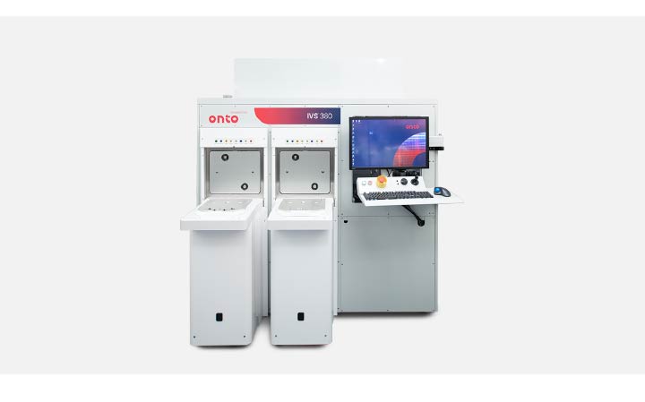
The IVS 380 System performs overlay, CD, and height metrology for 300mm wafers.

The KLA Surfscan SP 2 is a particle defect inspection system for semiconductor wafers.
The KLA .204 PSL Wafer is an 8-inch NIST-traceable reference wafer compatible with Surfscan 6xy0 and Sp1 particle counters.