Nanoscribe
Photonic Professional GT
The Nanoscribe Photonic Professional GT+ is a 3-dimension (3D) nanoprinter that uses two-photon absorption from an infrared (780 nm) femtosecond laser to expose and polymerize UV-sensitive photoresists. The highest resolution of the Nanoscribe Photonic Professional GT+ is below 200 nm lateral dimensions, achieved with the 63x objective in dip-in laser lithography (DILL) mode.[1]

What it is
How it works
The system uses two-photon polymerization with an infrared femtosecond laser to expose photoresist at the focal point. The focused beam induces polymerization only where the local intensity is high enough, which confines exposure to a small voxel inside the resist.[1][2][4]
The system combines a piezoelectric scanning stage with galvo-mirror beam steering. The piezo stage moves the substrate relative to the focus for high-precision placement, and the galvo mirrors deflect the focus laterally for faster scanning over larger regions.[4][2]
Where it fits in the process flow
The system sits in the lithography part of the microfabrication flow as a direct-write tool. The substrate is prepared with a suitable photoresist, the print file is loaded, the stage is aligned to the sample, and the structure is written before downstream development and cleaning steps.[2]
Applications
The system is used for optics, plasmonics, microfluidics, sensors, micro-robotics, biomimetics, and life-science structures. The tool is also used for micro- and nanoscale parts that require complex three-dimensional polymer geometry.[2][4][3]
The system uses UV-curable photoresists and supports direct laser writing with conventional and dip-in laser lithography modes. The available resist families include IP-Dip, IP-S, IP-Q, IP-Visio, and related formulations named for use with specific objectives and print modes.[2][1][3]
- two-photon polymerization
- photopolymerization of UV-sensitive photoresists
- DILL writing
- alignment on existing wafer/sample topography
Why won't it start?
Documented failure modes, common issues, and field considerations.
- The objectives are described as extremely sensitive and expensive.
- The equipment is described as sensitive to vibrations.
What do the numbers mean?
Power & electrical1
- Laser type
- 780 nm femtosecond fiber laser, 120 mW, 150 fs pulse duration, 80 MHz repetition rate, Class 3[2]
Wafer handling7
- Standard substrates
- quartz, silicon, ITO-coated glass, 170 µm-thick borosilicate, microscope slides up to 26 x 76 mm, 4 inch wafers, 2 inch wafers[1]
- Sample formats
- 25x25 mm² fused-silica, ITO-coated glass, silicon; 30 mm borosilicate; microscope slides up to 26x76 mm²; 4-inch and 2-inch wafers, thickness 350-550 µm[1]
- Substrates
- 25x25 mm fused silica, ITO-coated glass, silicon, 30 mm borosilicate, microscope slides, 4-inch and 2-inch wafers[1]
- Listed sample holders and substrates
- 25 x 25 mm² fused-silica substrate, 25 x 25 mm² ITO-coated glass substrate, 25 x 25 mm² silicon substrate, ∅ 30 mm thin borosilicate substrate, microscope slides up to 26 x 76 mm², 4 inch wafers, and 2 inch wafers[1]
Gas & chemistry1
- Photoresist compatibility
- UV-sensitive photoresists including standard i-line photoresists[1]
Optics & imaging36
- High resolution mode (3D SF) objective
- 63x NA1.4, 360um working distance, block-free printing field Ø 200 µm[1]
- Micro- to mesoscale mode (3D MF) objective
- 25x NA0.8, 380um working distance, block-free printing field Ø 400 µm[1]
- FAST macroscale mode (3D LF) objective
- 10x NA0.3, 700um working distance, block-free printing field Ø 1000 µm[1]
Performance3
Control & software3
Dimensions & facilities1
- Maximum structure height (various modes)
- 10x DILL (IP-Q): 8 mm; 25x DILL (IP-S): 3 mm; 63x DILL (IP-Dip): 3 mm; Oil immersion (63x, 170 µm glass): 150 µm[3]
Configuration & options19
Vintage & configurations
Documented models & variants
| Designation | Generation | Vintage | Changes | Source |
|---|---|---|---|---|
| Photonic Professional GT+ | — | — | The source describes GT+ as the model with multiple objectives, DILL configurations, oil-immersion options, and Describe software support. | epfl.ch[1] |
What does it need to run?
Site utility requirements, footprint, and infrastructure needed to install and operate this tool. Sourced from public records.
Where are the manuals?
Publicly hosted documents referencing this tool, linked at their original location. Hosted by the linked institutions — availability may change.
- Describe ManualManualepfl.ch
- Nanoscribe ManualManualepfl.ch
- ManualManualuic.edu
Generated from public-source data on file. Enter your email to access — nothing is published; details are routed privately.
Not publicly documented
Field notes
No research found yet — worked with this tool? Share what you know.
Frequently asked questions
What is the laser source wavelength of the Nanoscribe Photonic Professional GT?
What is the minimum feature size achievable?
With the 63x immersion objective, lateral dimensions below 200 nanometers can be achieved, and the minimum feature size is approximately 150 nanometers in X-Y and 800 nanometers in Z.[1][3]
Which photoresists are commonly used with the system?
Common photoresists include IP-Dip2, IP-S, IP-Q, IP-Visio, IP-PDMS, IP-L, and IPX formulations.[1][3][2]
Not publicly documented
The following facts about the Photonic Professional GT are absent from this record as of this revision. First-hand knowledge or a citation closes a gap; every submission is reviewed before publication.
No publicly documented production dates or lifecycle milestones (introduction, end of production, EOL) for the Photonic Professional GT are on record.
Answerable by: OEM historical records or a trade-press announcement
The control-system platform and OS era of the Photonic Professional GT are not on record.
Answerable by: an engineer who operated it or OEM installation records
The process node or technology generation of the Photonic Professional GT is not on record.
Answerable by: an OEM datasheet or a fab qualification report
No publicly documented compatible parts, consumables, or accessories for the Photonic Professional GT are on record.
Answerable by: an OEM parts catalog or a service engineer
Sources & citations
Sources (4)Every fact above is drawn from these public sources
- [1]epfl.ch — epfl.chepfl.ch
- [2]ncf.uic.edu — ncf.uic.eduncf.uic.edu
- [3]nanofab.utah.edu — nanofab.utah.edunanofab.utah.edu
- [4]Tool Details - Harvard CNS — cns1.rc.fas.harvard.educns1.rc.fas.harvard.edu
Last updated Oct 8, 2026.
Compare with similar tools
View all →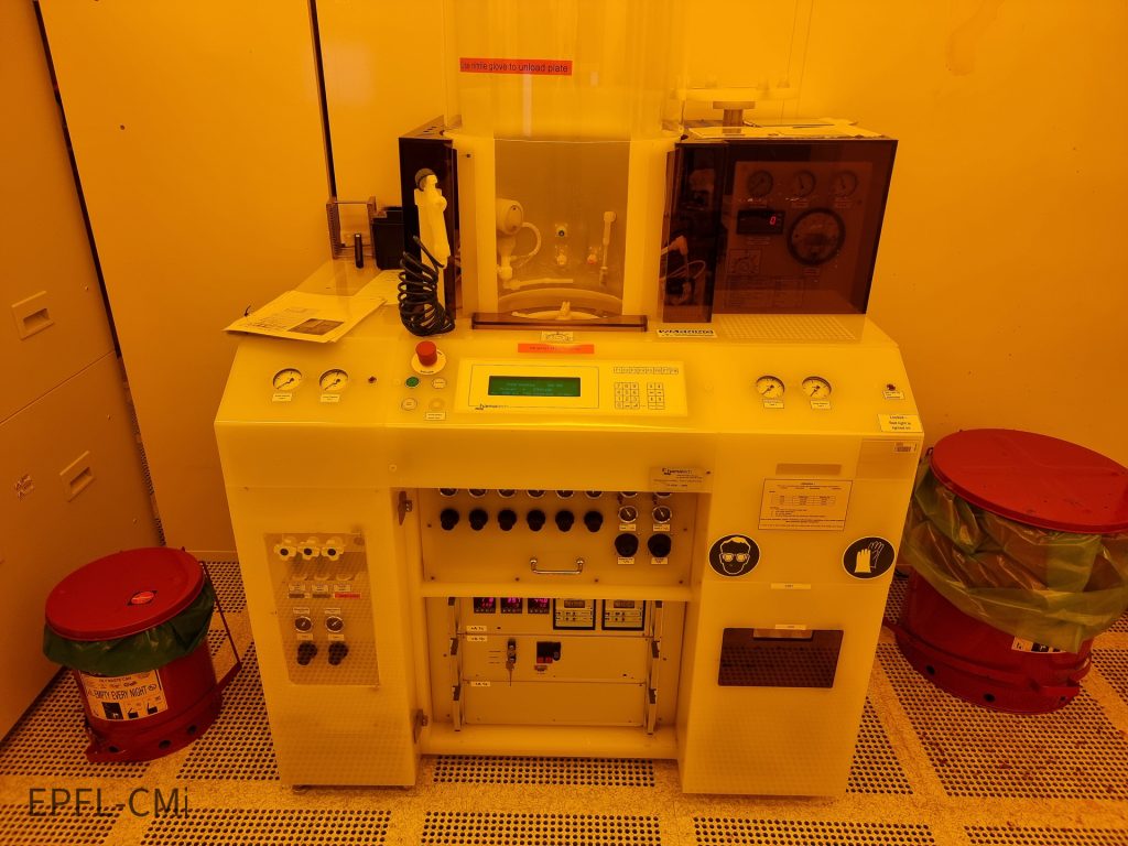
The Hamatech HMR900 is a mask processor for Cr-plate wet processing or cleaning.
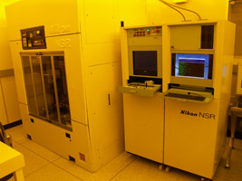
The Nikon NSR-1505G4 is a wafer stepper with 5x reduction for 5-inch reticles and 4-inch wafers, using g-line UV and providing better than 750 nm resolution and better than 150 nm alignment.
Brooks 017-0146-01 is a prealigner manufactured by Brooks.